
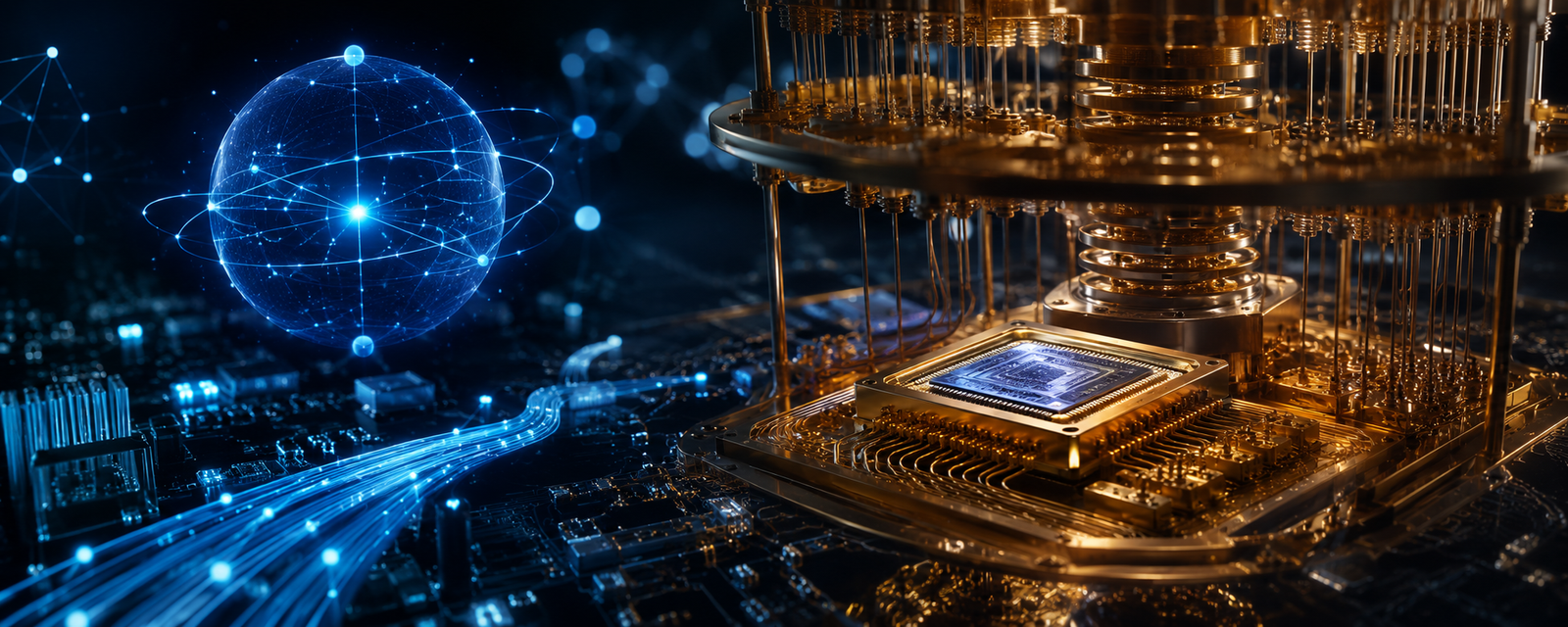
If you watched the cinematic classic Tron (1982) or its visually stunning sequel Tron: Legacy (2010), you were undoubtedly captivated by the glowing highways of light where digital information travels at the ultimate speed limit of the universe. In The Matrix (1999), the instantaneous breaching of master cryptographic ciphers personified the supreme power of advanced computing architectures. Across the Star Trek franchise, the starship Enterprise relies on optical isolinear chips that compute massive interstellar telemetry entirely immune to thermal dissipation. And in Alex Garland’s gripping series Devs (2020), a cryogenic vacuum-isolated quantum computer calculates the wavefunctions of the cosmos with such deterministic fidelity that it reconstructs the very fabric of physical reality.
For nearly eight decades, the modern digital civilization has operated under the undisputed empire of electrons traveling across doped silicon. From the invention of the point-contact transistor at Bell Laboratories in 1947 to contemporary artificial intelligence accelerators packing hundreds of billions of transistors, every milestone of computational progress has relied on shoving physical electrical charges through nanoscale copper wires etched onto monolithic silicon dies.
However, in 2026, classical microelectronics has collided head-on with an insurmountable physical and thermodynamic wall. Moore’s Law has officially reached its atomic exhaustion. At sub-atomic lithographic nodes of 2 nm and 1.4 nm, electrons succumb to quantum tunneling, leaking uncontrollably across gate dielectrics and generating catastrophic parasitic heat. To prevent the energetic stagnation of global computing, applied physics and computer science are spearheading the greatest hardware paradigm shift in human history: the transition from classical electronics to Quantum Computing, Silicon Photonics, and Terahertz Electronics, all shielded by Lattice-Based Post-Quantum Cryptography (PQC).
This master dossier serves as the Official Topic Hub of Reach Technocracy for the Frontier Hardware and Post-Silicon Computing ecosystem. Here, you will find the comprehensive theoretical, physical, and architectural backbone connecting all our deep-dive investigations: from qubit state mechanics and zero-resistance computing with light to 30-femtosecond quantum phase transitions and planetary cryptographic defenses against “Q-Day”.
Curated Reading Paths (Choose Your Track)
To extract maximum strategic value from this master guide based on your background and technical objectives, select your recommended reading path:
- 🟢 Track 1: The Tech Enthusiast & Visionary
- Focus: Core physical principles, pop-culture mental models, architectural shifts, and societal impact.
- Suggested Route: Introduction ➜ Chapters 1, 2, and 3 ➜ Fact vs. Sci-Fi Matrix ➜ Conclusion.
- 🔵 Track 2: The Systems & Software Engineer
- Focus: Quantum gate mechanics, Mach-Zehnder optical interferometry, lattice mathematics (LWE/SVP), and NIST FIPS standards.
- Suggested Route: Executive Takeaways ➜ Chapters 1 through 5 ➜ Access all linked In-Depth Spoke Essays.
- 🟣 Track 3: The Technology Executive & Deep-Tech Investor
- Focus: Datacenter thermal bottlenecks, the Co-Packaged Optics (CPO) transition, post-quantum enterprise migration, and the 2026–2035 Strategic Technology Roadmap.
- Suggested Route: Chapter Key Takeaways ➜ Chapter 1 ➜ Chapter 5 ➜ Chapter 7 (Roadmap) ➜ Download the Executive Dossier.
🧠 Fundamental Prerequisites & Key Concepts
- Qubit & Quantum Superposition: The fundamental quantum information unit described by the state vector |ψ⟩ = α|0⟩ + β|1⟩ (where |α|² + |β|² = 1), maintaining a continuous linear superposition of states until physical measurement.
- Quantum Entanglement: A non-local quantum correlation where multiple qubits share an inseparable joint state. For N entangled qubits, the computational state space scales exponentially to 2^N simultaneous complex amplitudes.
- Mach-Zehnder Interferometry (MZI) & Silicon Photonics: Integrated optical circuits that manipulate laser phase shifts across silicon waveguides to execute tensor matrix multiplications at the speed of light via constructive and destructive interference.
- Lattice-Based Cryptography (PQC): Post-quantum mathematical algorithms rooted in NP-hard geometric lattice problems in 500 to 1,000-dimensional vector spaces (SVP and LWE), intrinsically immune to Shor’s algorithm.
- Terahertz (THz) Electronics & 30 Femtoseconds: An ultra-high-frequency regime (0.1 to 10 THz) where optoelectronic state transitions occurring in 30 femtoseconds (30 × 10⁻¹⁵ s) decouple electron dynamics from thermal lattice vibrations (phonons).
- Q-Day & Harvest Now, Decrypt Later (HNDL): The milestone when fault-tolerant quantum computers break classical public-key cryptography (RSA/ECC). HNDL represents the active interception and archiving of encrypted data today for retroactive quantum decryption tomorrow.
⏳ Dynamic Timeline of Quantum and Post-Silicon Hardware
- Phase 1 (1900–1994: Theoretical Foundations & Shor’s Breakthrough)
- 1947: Invention of the point-contact transistor at Bell Labs, inaugurating the silicon era.
- 1981: Richard Feynman proposes quantum computing to simulate quantum mechanical systems naturally.
- 1994: Peter Shor publishes his polynomial-time quantum algorithm for integer factorization and discrete logarithms.
- Phase 2 (1995–2023: The NISQ Era & Prototype Systems)
- 2005: Collapse of Dennard Scaling in microprocessors, locking commercial CPU clocks at 4–5 GHz.
- 2016: NIST launches the global Post-Quantum Cryptography Standardization Project.
- 2019–2023: Demonstrations of statistical quantum supremacy on Noisy Intermediate-Scale Quantum (NISQ) devices by Google and IBM.
- Phase 3 (2024–2026: The Inflection Point — CPO, NIST Standards & Neutral Atoms)
- August 2024: NIST ratifies the first official global PQC standards (FIPS 203 ML-KEM, FIPS 204 ML-DSA, FIPS 205 SLH-DSA).
- 2025: Hyperscale deployment of Co-Packaged Optics (CPO) by TSMC, NVIDIA, and Broadcom in 51.2 Tbps and 102.4 Tbps switches.
- 2026: Demonstration of neutral-atom quantum processors (QuEra/Harvard) executing logical algorithms with dozens of error-corrected qubits; 30-fs optical THz switching.
- Phase 4 (2027–2035: The Post-Silicon Horizon — Fault Tolerance & Quantum Networks)
- 2027–2029: Emergence of commercial hybrid supercomputers integrating photonic AI accelerators with 1,000-logical-qubit coprocessors.
- 2030–2032: Mandatory global completion of enterprise PQC migration; deployment of metropolitan quantum repeater networks.
- 2033–2035: Full realization of universal Fault-Tolerant Quantum Computing (FTQC) breaking legacy 2048-bit RSA keys (Q-Day horizon).
1. The End of the Electron Empire: The Collapse of Moore’s Law and the Thermal Wall
📌 Chapter Key Takeaways:
- Dennard Scaling collapsed in 2005, freezing microprocessor clock frequencies at 4–5 GHz due to uncontrollable Joule heating.
- Below 3 nm lithography, sub-atomic quantum tunneling causes severe static current leakage across atomic gate dielectrics.
- The Von Neumann Memory Wall squanders up to 80% of datacenter AI energy exclusively on shuttling electrical charges across copper interconnects.
The Exhaustion of Silicon and the Collapse of Dennard Scaling
For four decades, the relentless expansion of the digital economy was propelled by Dennard Scaling (formulated by Robert H. Dennard in 1974): as MOSFET transistors shrank in physical dimensions, their operating voltage scaled down proportionally, maintaining a constant power density (Watts per square centimeter) while permitting exponential increases in clock frequency.
Around 2005, this physical relationship broke down permanently. Operating voltages hit a fundamental physical threshold of ~0.7 Volts, beneath which thermal noise triggers stochastic switching errors. Unable to lower the voltage further, semiconductor architects were forced to freeze clock speeds in the 4.0 GHz to 5.0 GHz range to prevent silicon chips from literally melting. Every electrical current traversing metallic wires encounters ohmic resistance and phonon scattering, transforming valuable energy into parasitic waste heat governed by Joule’s Law (P = I² · R).
Quantum Tunneling and the Von Neumann Memory Wall
In contemporary manufacturing nodes (such as 3 nm, 2 nm, and 1.4 nm Gate-All-Around / Nanosheet architectures from TSMC and Intel), insulating gate dielectrics measure merely a few atomic layers of silicon dioxide or high-k dielectrics. At this scale, electrons cease to behave as localized Newtonian particles and manifest as quantum probabilistic wavefunctions. Through quantum tunneling, electrons leak directly through the potential barrier when the transistor is switched off, generating massive static leakage currents that drain power even when idle.
Simultaneously, the classical Von Neumann Architecture—which physically isolates the arithmetic logic unit (GPU/CPU) from volatile working memory (DRAM/HBM)—has formed the notorious Memory Wall. In large-scale generative AI workloads, over 80% of total electrical energy is dissipated merely dragging bits across nanoscale copper traces on the printed circuit board rather than performing actual mathematical operations. To avert the total stall of computing, electrons must be superseded by coherent light and quantum wavefunctions.
🔬 IN-DEPTH TECHNICAL ESSAY:
To explore the mathematical physics of silicon’s thermal wall and the transition to optical conductors, read our complete analysis:
👉 Optical Chips and Computing with Light: Shattering the Silicon Limit and Moore’s Law
2. The Mechanics of Qubits: Superposition, Entanglement, and the Quantum Computer Race
📌 Chapter Key Takeaways:
- Quantum state spaces scale exponentially as 2^N through the physical principles of linear superposition and non-local entanglement.
- Five competing physical qubit modalities are in a global race: superconducting transmons, trapped ions, neutral atoms, photonics, and topological qubits.
- Industrial utility demands Quantum Error Correction (QEC) via Surface Codes to synthesize stable logical qubits from thousands of noisy physical qubits.
The Physics of Superposition and the Bloch Sphere
Unlike a classical bit constrained to binary states of 0 or 1, a qubit exists as a continuous linear superposition of orthogonal basis states represented as |ψ⟩ = α|0⟩ + β|1⟩, where α and β are complex probability amplitudes satisfying |α|² + |β|² = 1. Geometrically, any pure single-qubit state corresponds to a point on the surface of the three-dimensional Bloch Sphere, navigated continuously via unitary quantum logic gates (Hadamard, Pauli-X, Y, Z, and Phase Shift rotations) prior to projective measurement.
The Exponential Power of Entanglement
When multiple qubits interact, they form an entangled quantum state whose joint wavefunction cannot be factored into individual subsystem states. For a system of N entangled qubits, the computational state space spans 2^N simultaneous complex probability amplitudes:
- 50 Qubits: Simultaneously evaluate over 1.12 × 10¹⁵ states, matching the memory capacity of premier classical supercomputers.
- 300 Qubits: Process 2³⁰⁰ ≈ 2 × 10⁹⁰ states concurrently—a number exceeding the total estimated subatomic particles in the observable universe.
This massive parallelism enables revolutionary quantum algorithms, including Grover’s Algorithm for quadratic database search acceleration (O(√N)) and Shor’s Algorithm for exponential prime factorization (O((log N)³)).
The Five Physical Qubit Modalities
- Superconducting Circuits (Transmons): Pioneered by IBM (Heron, Condor) and Google Quantum AI (Sycamore). Micro-lithographed planar Josephson junctions operating at dilution refrigerator temperatures of 15 millikelvin. Strength: nanosecond-fast gate speeds. Challenge: brief coherence times (hundreds of microseconds) and complex cryogenic plumbing.
- Trapped Ions: Championed by IonQ and Quantinuum. Chains of individual Ytterbium (Yb+) or Barium (Ba+) ions suspended in ultra-high vacuum RF Paul traps and manipulated via focused laser beams. Strength: pristine gate fidelities exceeding 99.9%. Challenge: slower millisecond gate operations.
- Neutral Atoms in Optical Tweezers: Spearheaded by QuEra Computing, Harvard University, and MIT. Hundreds of uncharged Rubidium or Cesium atoms trapped in 2D/3D focal laser grids and excited to giant Rydberg states for dipole-blockade gate operations. Strength: exceptional geometric reconfigurability and rapid synthesis of dozens of error-corrected logical qubits.
- Quantum Photonics: Advanced by PsiQuantum and Xanadu. Qubits encoded directly onto single photons traveling through room-temperature silicon-on-insulator waveguides. Strength: natural networking compatibility and room-temperature operation. Challenge: probabilistic photon generation and photon-photon gate synthesis.
- Topological Majorana Qubits: Pursued by Microsoft Quantum. Non-Abelian anyon quasi-particles residing in hybrid semiconductor-superconductor nanowires, providing hardware-intrinsic topological protection against environmental noise.
Quantum Error Correction (QEC) and Logical Qubits
The primary barrier to scalable quantum advantage is Quantum Decoherence: environmental thermal fluctuations, electromagnetic noise, and material impurities disrupt fragile quantum superpositions within microseconds. Overcoming the noisy NISQ era requires Quantum Error Correction (QEC).
Through Surface Codes, hundreds or thousands of physical qubits are entangled into a single fault-tolerant Logical Qubit. By measuring multi-qubit parity stabilizers without collapsing the underlying data state, QEC syndromes detect and correct bit-flip (X) and phase-flip (Z) errors in real time, reducing logical error rates exponentially.
🔬 IN-DEPTH TECHNICAL ESSAYS:
To master the foundational physics of qubits and the engineering architectures solving quantum decoherence, read our complete analyses:
👉 What Is Quantum Computing and How Does It Work Simply?
👉 The Major Challenges of Quantum Computing (and How Science Plans to Solve Them)
3. Photonic Processors: How Light Computes Frictionless at the Speed of the Cosmos
📌 Chapter Key Takeaways:
- Photons possess zero rest mass and zero electrical charge, eliminating resistive Joule dissipation (P = 0) during signal propagation.
- Programmable 2D meshes of Mach-Zehnder Interferometers (MZIs) execute tensor matrix multiplications at the time-of-flight speed of light (<100 ps).
- Co-Packaged Optics (CPO) directly bridges optical engines to processor dies, slashing datacenter networking power consumption by 30% to 40%.
The Physics of Photons and Silicon Photonics
To accelerate intensive AI workloads without collapsing municipal power grids, Optical Processing Units (OPUs) replace electron transport with guided photons:
- Zero Electrical Charge (q = 0): Photons do not experience Coulomb repulsion and generate zero ohmic resistive friction (P = I² · R = 0).
- Relativistic Speed of Propagation: Photons traverse silicon waveguides (refractive index n ≈ 3.45) at ~87,000 km/s, completing multi-layer tensor calculations with pure time-of-flight picosecond latencies.
- Wavelength Division Multiplexing (WDM): Multiple distinct optical carrier wavelengths travel simultaneously through a single sub-micron silicon waveguide without mutual cross-talk, multiplying channel bandwidth by orders of magnitude.
How Light Calculates: Mach-Zehnder Interferometers (MZIs)
The core computational engine of a photonic processor is the Mach-Zehnder Interferometer (MZI). Coherent laser light enters a 50:50 directional beam splitter, dividing into two parallel waveguide arms. Applied electric voltages or micro-heaters modulate the refractive index in one arm, introducing a precise phase shift Δθ. When the beams recombine at the output coupler, they interfere constructively or destructively.
By cascading hundreds or thousands of MZIs into programmable 2D triangular or rectangular meshes (the Reck or Clements architectures), the optical circuit mathematically implements arbitrary unitary matrix transformations. Vector inputs encoded as light pulses pass through the mesh, and General Matrix Multiplications (GEMM / MatMul) are resolved instantaneously in the optical domain as the light traverses the chip in under 100 picoseconds, consuming up to 95% less energy than high-end GPUs.
Co-Packaged Optics (CPO) and the Industrial Ecosystem
- Co-Packaged Optics (CPO): Industrial consortiums led by TSMC (COUPE technology), NVIDIA, Broadcom, and Intel are transitioning optical transceivers from rack faceplates directly onto the advanced 2.5D/3D multi-die package (CoWoS). By eliminating inches of high-frequency copper traces, CPO reduces interconnect energy consumption by 30% to 40% in 51.2 Tbps and 102.4 Tbps network switches.
- Lightmatter: The MIT spin-out has developed the Envise photonic AI inference processor and the Passage wafer-scale optical interconnect platform, interconnecting heterogeneous compute dies across a continuous silicon photonics wafer at terabits per second.
- Celestial AI: Developing the Photonic Fabric architecture to optically disaggregate compute and high-bandwidth memory (HBM) pools across datacenters with native on-chip latencies.
🔬 IN-DEPTH TECHNICAL ESSAY:
To explore the engineering mechanics of silicon photonics, Mach-Zehnder meshes, and Co-Packaged Optics, read our dedicated investigation:
👉 Optical Chips and Computing with Light: Shattering the Silicon Limit and Moore’s Law
4. The 30-Femtosecond Frontier and the Awakening of Terahertz Electronics
📌 Chapter Key Takeaways:
- Ultrashort 30-femtosecond (30 × 10⁻¹⁵ s) optical laser pulses reconfigure electronic quantum states before atomic lattice nuclei can vibrate.
- Pump-probe spectroscopy and tr-ARPES capture hidden non-equilibrium states of matter and generate photonic time crystals.
- Femtosecond optoelectronic switching bridges the “THz Gap”, unlocking 1,000x faster processing and 1 Tbps 6G/7G wireless communications.
Electronic Lattice Decoupling in 30 Femtoseconds
One femtosecond is 10⁻¹⁵ seconds. In 30 femtoseconds, light travels a mere 9 micrometers—roughly the width of a single human red blood cell. On this extreme timescale, the classical Born-Oppenheimer Approximation collapses:
- Heavy atomic nuclei and lattice vibrations (phonons) operate sluggishly across hundreds of femtoseconds to picoseconds due to nuclear inertia.
- Lightweight valence electrons respond almost instantaneously to coherent electromagnetic fields within tens of femtoseconds.
- By striking a correlated quantum material with a 30-fs laser pulse, electrons reorganize into entirely new periodic quantum bonding states before the atomic nuclei can physically move, switching material conductivity without generating thermal phonon friction.
Pump-Probe Spectroscopy, Photonic Time Crystals, and the THz Gap
Using Pump-Probe Spectroscopy and time-resolved ARPES (tr-ARPES), physicists film the evolution of electronic wavefunctions frame-by-frame, uncovering Hidden States and synthesizing Photonic Time Crystals (PTCs) whose refractive index oscillates periodically in time, amplifying electromagnetic signals exponentially.
This breakthrough directly closes the historical Terahertz Gap (0.1 to 10 THz):
- A 1 THz electromagnetic wave cycles in 1,000 femtoseconds. A 30-fs transition completes in a tiny fraction of a single wave cycle.
- Enables solid-state optoelectronic switches operating in the Multi-Terahertz domain—over 1,000 times faster than state-of-the-art silicon CMOS.
- Provides carrier frequencies for 6G and 7G wireless telecommunications delivering over 1 Terabit per second (1 Tbps).
- Executes ultrafast quantum logic gates in femtoseconds before thermal decoherence can degrade qubit fidelity.
🔬 IN-DEPTH TECHNICAL ESSAY:
To explore the condensed matter physics of non-equilibrium states, ultrafast tr-ARPES spectroscopy, and terahertz switching, read our complete analysis:
👉 The 30-Femtosecond Frontier: How Quantum Manipulation of Matter by Light Unlocks the Terahertz Era
5. Q-Day and Lattice Cryptography: The Post-Quantum Shield for the Global Internet
📌 Chapter Key Takeaways:
- Shor’s Algorithm running on fault-tolerant quantum hardware will completely dissolve RSA and Elliptic Curve Cryptography (ECC) within minutes.
- The Harvest Now, Decrypt Later (HNDL) intelligence doctrine poses an immediate active threat to confidential data recorded today.
- Lattice-Based Cryptography (NIST FIPS 203 ML-KEM and FIPS 204 ML-DSA) provides unbreakable geometric defenses in high-dimensional vector spaces.
Shor’s Algorithm and the Harvest Now, Decrypt Later Threat
Modern global digital security—protecting HTTPS/TLS 1.3, banking networks, identity systems, and state defense infrastructure—relies on trapdoor mathematical functions: integer factorization of giant primes (RSA) or the discrete logarithm problem over elliptic curves (ECC). In 1994, Peter Shor demonstrated that a fault-tolerant quantum computer executing the Quantum Fourier Transform solves these problems in polynomial time (O((log N)³)).
The most pressing danger is not hypothetical future hardware, but the active intelligence doctrine of Harvest Now, Decrypt Later (HNDL): foreign adversaries and cyber consortiums are actively intercepting and storing petabytes of encrypted transoceanic communications today, intending to decrypt diplomatic records, medical databases, and critical intellectual property the moment quantum supercomputers achieve commercial scale on Q-Day.
The Fortress of High-Dimensional Lattices and NIST FIPS Standards
Post-Quantum Cryptography (PQC) replaces number-theoretic trapdoors with high-dimensional Euclidean geometry: Lattices in 500 to 1,000 dimensions. Security is grounded in worst-case NP-hard geometric problems, including the Shortest Vector Problem (SVP) and Learning With Errors (LWE), which contain no periodic abelian group structures that Shor’s algorithm can exploit.
In August 2024, the U.S. National Institute of Standards and Technology (NIST) officially ratified the global cryptographic standards for the 21st century:
- ML-KEM (FIPS 203 / CRYSTALS-Kyber): Primary standard for key encapsulation mechanisms in web sessions, VPNs, and TLS 1.3 handshakes.
- ML-DSA (FIPS 204 / CRYSTALS-Dilithium): Primary standard for digital signatures, PKI certificates, and operating system firmware verification.
- SLH-DSA (FIPS 205 / SPHINCS+): Stateless hash-based digital signatures serving as an indestructible secondary mathematical fallback.
Leading technology platforms—including Google Chrome, Cloudflare, and Apple iMessage (PQ3)—have already deployed Hybrid Key Exchange (X25519 + ML-KEM-768), combining classical elliptic curves with lattice cryptography to guarantee seamless forward secrecy during the global migration.
🔬 IN-DEPTH TECHNICAL ESSAY:
To understand the high-dimensional geometry of lattices, Shor’s algorithm matrix transformations, and the NIST FIPS migration standards, read our complete analysis:
6. Fact vs. Hypothesis vs. Science Fiction Matrix
To establish rigorous epistemological boundaries across the post-silicon landscape, the following matrix delineates proven laboratory reality, active scientific hypotheses, and speculative science fiction myths:
| Technology Dimension | 🟢 Proven Fact (State of the Art in 2026) | 🟡 Scientific Hypothesis (Active Research) | 🔴 Science Fiction & Popular Myths |
|---|---|---|---|
| Quantum Computing | Physical processors exceeding 1,000 raw qubits (IBM Heron) and dozens of logical qubits running Surface Code error correction (QuEra/Harvard). | Scaling to 10,000 fault-tolerant logical qubits for exact molecular drug simulation and room-temperature superconductor design. | Quantum personal computers replacing desktop PCs and smartphones for everyday web browsing or gaming. |
| Silicon Photonics | Co-Packaged Optics (CPO) deployed in 51.2 Tbps datacenter switches; MZI optical meshes executing tensor matrix multiplication with <100 ps latency. | All-optical non-linear logic gates replacing digital silicon GPUs for the entirety of frontier AI inference workloads. | Photonic chips operating entirely without analog-to-digital converters or persistent electronic memory storage. |
| Terahertz Electronics | Quantum optoelectronic switching in 30 femtoseconds via pump-probe spectroscopy fully decoupled from atomic lattice phonons. | Commercial solid-state transistors maintaining stable, uncooled 1 THz operation in ambient consumer electronics and 6G infrastructure. | Infinite-speed microprocessors violating the speed of light in vacuum and fundamental quantum causality bounds. |
| Post-Quantum Cryptography | Official ratification of NIST standards FIPS 203 (ML-KEM) and FIPS 204 (ML-DSA); active deployment in Google Chrome and Apple iMessage. | Universal 100% migration of global banking and sovereign defense networks completed prior to fault-tolerant Q-Day. | Flawless cryptographic ciphers universally immune to all side-channel attacks, implementation bugs, and human error. |
| Bio-Quantum Substrates | Synthetic DNA storing 215 Petabytes/gram; living human 3D neural organoids integrated on microelectrode arrays (MEAs) executing learning tasks. | Commercial bio-hybrid cloud servers running continuous AI model training consuming less than 20 Watts of biological power. | Spontaneous sentient artificial consciousness emerging inside in vitro Petri dishes (e.g., Dune Mentats or The Matrix pods). |
7. Strategic Frontier Hardware Roadmap (2026–2035)
- 2026–2027: Hyperscale Co-Packaged Optics & Mandatory PQC Adoption
- Widespread deployment of 51.2 Tbps and 102.4 Tbps CPO optical switch engines in tier-1 hyperscale datacenters (TSMC, NVIDIA, Broadcom), cutting networking power by 30%.
- Mandatory enforcement of NIST FIPS 203 (ML-KEM) and FIPS 204 (ML-DSA) across federal agencies in the US, EU, and NATO member states.
- Demonstration of early commercial quantum utility in quantum chemistry using 256-logical-qubit neutral-atom arrays.
- 2028–2030: Fault-Tolerant Logical Qubits & Photonic AI Accelerators
- Commercial cloud access to Surface-Code-corrected quantum computing clusters exceeding 1,000 fault-tolerant logical qubits.
- Production deployment of wafer-scale optical interconnects (Passage/Photonic Fabric) slashing LLM memory bandwidth bottlenecks by 70%.
- Standardization and industrial certification of sub-THz (100–300 GHz) transceivers for preliminary 6G wireless infrastructure.
- 2031–2035: Q-Day, Universal Quantum Advantage & The Quantum Internet
- Quantum supercomputers reach the operational scale required to crack legacy RSA-2048 keys (the full Q-Day threshold).
- Intercontinental quantum repeater networks operational, enabling entanglement distribution and global Quantum Key Distribution (QKD).
- Integration of 30-femtosecond laser-driven solid-state switches into specialized ultra-high-speed scientific supercomputers.
Conclusion: The Dawn of Post-Silicon Hardware
The history of modern computing was forged on the confinement of electrons within inorganic crystalline silicon. This monolithic formula unlocked microprocessors, personal computing, the internet, and modern artificial intelligence. Yet the unforgiving laws of physics—Dennard collapse, quantum tunneling, and the thermodynamic power wall—have brought this golden era to its inevitable conclusion.
The ongoing transition to post-silicon hardware marks an ontological turning point in computing:
- In Quantum Computing, we compute in the native language of physical reality—superposition, entanglement, and unitary probability amplitudes.
- In Silicon Photonics, dense matrix arithmetic transforms into beams of coherent light propagating through crystal waveguides at the speed of the cosmos with zero resistive heat.
- In Femtosecond and Terahertz Physics, we shatter the inertia of atoms, manipulating electronic phases in timescales where thermal time itself appears frozen.
- In Lattice-Based Cryptography, we erect unbreakable geometric fortresses across thousand-dimensional vector spaces to preserve human privacy in the post-quantum era.
At Reach Technocracy, we remain dedicated to standing at the absolute vanguard of this transformation—opening the hood on cryogenic dilution refrigerators, photonic foundries, and advanced condensed matter laboratories to deliver rigorous, actionable clarity on the technologies shaping the future of intelligence.
Frequently Asked Questions (FAQ)
1. What is the fundamental difference between a classical computer and a quantum computer?
A classical computer processes discrete binary bits (0 or 1) through voltage-gated silicon transistors. A quantum computer uses quantum bits (qubits), which harness the physical principles of linear superposition (existing in a linear combination of 0 and 1 simultaneously) and quantum entanglement. This enables an N-qubit quantum processor to manipulate 2^N complex states simultaneously, providing exponential speedups for specialized problems in quantum chemistry, materials science, optimization, and integer factorization.
2. What is the thermal wall of silicon and why has Moore’s Law ended?
The thermal wall (or Power Wall) arose from the breakdown of Dennard Scaling around 2005. Below 3 nm lithography, operating voltages cannot be lowered below ~0.7V without causing switching noise errors. The resulting ohmic resistance from moving trillions of electrons generates massive Joule heat (P = I² · R), freezing clock speeds at 4–5 GHz. Additionally, sub-atomic quantum tunneling causes electrons to leak through atomic gate dielectrics even when switched off, halting traditional silicon scaling.
3. How do silicon photonic chips execute AI calculations at the speed of light?
Silicon photonic chips replace electrical currents with infrared laser light traveling through etched silicon waveguides. Matrix multiplications for neural networks are executed passively within programmable 2D meshes of Mach-Zehnder Interferometers (MZIs). By applying micro-voltages to phase shifters, light waves interfere constructively and destructively, solving matrix arithmetic during the physical time-of-flight of photons through the chip (<100 picoseconds) with near-zero heat dissipation.
4. What is “Q-Day” and why are organizations migrating to Lattice-Based Cryptography?
Q-Day is the point in time when fault-tolerant quantum computers running Shor’s Algorithm can break legacy public-key encryption (RSA and ECC) in minutes. Because malicious actors are already recording encrypted network traffic today to decrypt later (Harvest Now, Decrypt Later), NIST officially standardized Lattice-Based Cryptography (FIPS 203 ML-KEM and FIPS 204 ML-DSA) in August 2024. These algorithms rely on NP-hard geometric problems in 500 to 1,000 dimensions that quantum computers cannot solve efficiently.
5. What is the significance of the 30-femtosecond frontier in ultrafast electronics?
One femtosecond is 10⁻¹⁵ seconds. On a 30-femtosecond timescale, light travels just 9 micrometers. Striking quantum materials with 30-fs laser pulses reconfigures electronic states before heavy atomic nuclei (phonons) can physically vibrate, breaking the Born-Oppenheimer approximation. This enables lossless optoelectronic switching in the Terahertz domain (0.1 to 10 THz)—1,000 times faster than silicon—paving the way for 1 Tbps 6G/7G wireless networks and ultrafast quantum logic gates.
Continue Exploring the Frontier of Science and Technology
- What Is Quantum Computing and How Does It Work Simply? — Fundamental principles of qubits, superposition, and the Bloch Sphere.
- The Major Challenges of Quantum Computing (and How Science Plans to Solve Them) — Phase noise, thermal decoherence, and Surface Code quantum error correction.
- Optical Chips and Computing with Light: Shattering the Silicon Limit and Moore’s Law — Photonic AI accelerators, Mach-Zehnder meshes, and Co-Packaged Optics.
- The 30-Femtosecond Frontier: How Quantum Manipulation of Matter by Light Unlocks the Terahertz Era — Hidden states of matter, photonic time crystals, and lossless THz switching.
- Lattice-Based Cryptography: The Mathematical Shield That Will Save the Internet from the Quantum Apocalypse — Shor’s algorithm, high-dimensional lattice geometry, and NIST FIPS standards.
- Hub 1: The Definitive Guide to Artificial Intelligence — From Language Models to Multi-Agent Systems, Physical AI, and AGI — Explore our sister master guide on autonomous agents, world models, and synthetic cognition.