
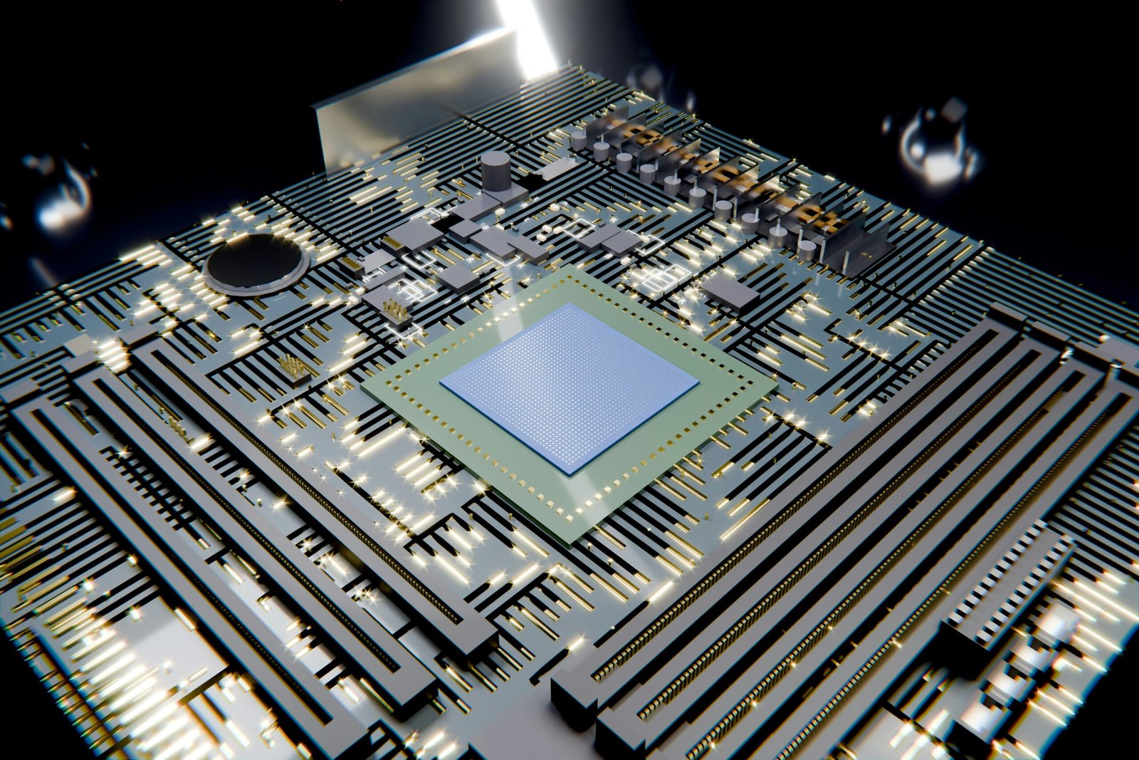
If you watched the groundbreaking sci-fi classic Tron (1982) or its visually stunning sequel Tron: Legacy (2010), you undoubtedly remember its mesmerizing depiction of digital circuits: glowing neon highways of pure light where data does not travel as sluggish electricity, but as radiant photonic pulses cutting through cyberspace at the absolute speed limit of the universe.
If your cinematic imagination belongs to the Star Wars universe, the legendary lore of Kyber crystals focusing pure photonic energy evokes that same primal human fascination with the transformative power of light. Or consider Star Trek, where the starship Enterprise’s main computer utilizes “isolinear optical circuitry” to process interstellar telemetry without electronic bottlenecks.
For nearly eighty years, the architecture of modern digital civilization has rested upon a single technological dogma: the absolute reign of electrons flowing through silicon. From the invention of the point-contact transistor at Bell Labs in 1947 to today’s multi-billion-transistor smartphone chips and AI accelerators, all computational progress has relied upon pushing trillions of physical electrons through microscopic copper interconnects etched into silicon wafers.
However, the electronic paradigm has officially slammed into an insurmountable thermodynamic and physical wall. The legendary Moore’s Law — the golden rule dictating that transistor counts on a chip would double every two years — is effectively dead. Transistors have shrunk to atomic dimensions of 2 and 3 nanometers, where electrons succumb to the bizarre effects of quantum mechanics, leaking across silicon barriers and generating catastrophic waste heat that threatens to cap the expansion of global artificial intelligence data centers.
To avert this computational bottleneck, materials science and computer engineering are driving the most profound hardware paradigm shift in history: replacing physical electrons with photons (particles of light). Welcome to the era of Silicon Photonics and Optical Processing Units (OPUs).
In this deep dive from Reach Technocracy, we dissect the fundamental physics and microengineering transforming global computing. We will explore why electronic semiconductors have reached their hard physical limits, examine how light executes complex neural network matrix math at the speed of light without resistive heat, explore the foundational building blocks of an optical processor (such as Mach-Zehnder Interferometers), and evaluate the vanguard enterprises building the photonic supercomputing of the 21st century.
1. The Electronic Dead-End: Heat, Resistance, and the Death of Moore’s Law
To appreciate the urgency of optical computing, we must first examine why conventional electronic semiconductors are suffocating under the laws of classical physics.
A standard electronic microprocessor (such as modern CPUs and GPUs) is composed of tens of billions of complementary metal-oxide-semiconductor (CMOS) transistors. Each transistor functions as a microscopic electronic switch: when voltage is applied, electrons flow through a silicon channel (representing binary 1); when voltage ceases, electron flow is halted (representing binary 0).
For decades, the semiconductor industry accelerated performance simply by miniaturizing these switches. Today, however, that scaling paradigm has encountered three fatal physical barriers:
The Thermal Ceiling and the End of Dennard Scaling
As electrons travel through conductive silicon and copper channels, they continuously collide with the host material’s atomic crystal lattice. This resistive friction dissipates electrical energy as immense waste heat (Joule Heating). Nearly two decades ago, microprocessor clock speeds stalled in the 4 to 5 GHz window because driving electrons any faster would literally melt the silicon substrate. Today, hyperscale artificial intelligence data centers consume nearly as much electrical power cooling servers as they do executing computational workloads.
The Von Neumann Memory Wall
In modern computing architectures, the primary consumer of execution time and energy is not the mathematical calculation itself, but the physical transport of data between the processing core (GPU) and high-bandwidth memory (RAM) across metallic copper traces. This continuous electronic traffic consumes up to 80% of total system power and creates a severe data bottleneck.
Sub-Atomic Quantum Tunneling
Cutting-edge semiconductor nodes feature transistor gate dimensions of just 2 to 3 nanometers — equivalent to the width of roughly a dozen aligned silicon atoms. At this sub-nanometer scale, electrons cease behaving purely as classical particles and exhibit probabilistic quantum wave characteristics: they undergo Quantum Tunneling, spontaneously leaking across closed transistor gates. This causes chronic current leakage, signal corruption, and operational instability.
2. The Physics of Photons: Why Light is the Ultimate Information Carrier
The technological answer to these electronic constraints lies in replacing the fundamental information carrier: substituting charged, massive electrons with photons — massless particles of pure light.
Quantum electrodynamics endows photons with unmatched physical advantages for computational architectures:
- Cosmic Speed of Propagation: While the drift velocity of physical electrons through copper wire is merely millimeters per second, photons travel at the cosmic speed limit: 300,000 km/s in a vacuum and roughly 200,000 km/s inside silicon waveguides, collapsing computational propagation latency to picoseconds.
- Zero Electrical Charge and Zero Joule Heating: Because photons carry zero electric charge and zero rest mass, they experience zero ohmic friction within silicon crystal lattices and do not interact electrostatically with neighboring photons. Two beams of light can cross the exact same physical space without colliding, distorting, or generating thermal heat.
- Wavelength Division Multiplexing (WDM): On a copper trace, only a single electrical voltage state can exist at any given instant. In silicon photonics, however, Wavelength Division Multiplexing allows engineers to inject dozens or hundreds of distinct laser frequencies (colors of light) simultaneously into a single microscopic waveguide. Each color carries an independent data stream in parallel with zero cross-talk, multiplying interconnect bandwidth by orders of magnitude.
3. Anatomy of an Optical Processor: How Does Light Calculate?
A common question naturally arises: “Light travels fast, but how can beams of light actually execute mathematical operations like multiplication and addition without transistors?”
The answer lies in the wave mechanics of Optical Interference.
An Optical Processing Unit (OPU) leverages micro-scale photonic integrated circuits fabricated on standard silicon wafers using deep-ultraviolet lithography:
Silicon Waveguides (Microscopic Light Channels)
These are sub-micron transparent silicon channels clad in silicon dioxide with a lower refractive index. They function as on-chip microscopic optical fibers, trapping and guiding laser light via total internal reflection with minimal propagation loss.
Electro-Optic Modulators and Micro-Ring Resonators
These act as system translators: receiving digital electronic voltage streams and modulating the phase or amplitude of continuous-wave laser beams at tens of gigahertz, converting numbers into photonic pulses.
Mach-Zehnder Interferometers (MZIs): The Engines of Optical Math
The Mach-Zehnder Interferometer (MZI) is the fundamental arithmetic logic unit of photonic computing. It operates by splitting an incoming beam of coherent laser light into two parallel optical paths:
- An electro-optic or thermal phase shifter applies a precise phase delay to one of the light paths.
- When the two beams recombine at the output coupler, the light waves undergo Constructive Interference (adding amplitudes) or Destructive Interference (subtracting amplitudes).
- The resulting output optical intensity directly represents the exact mathematical product of a multiplication and addition operation!
Matrix Multiplication at the Speed of Light
Photonic processing is exceptionally suited for Artificial Intelligence workloads because over 90% of large language model computation (such as GPT-4, Claude, and Gemini) consists of General Matrix Multiplications (GEMM / MatMul).
While a conventional silicon GPU must toggle billions of transistors across hundreds of clock cycles to compute heavy matrix math — burning hundreds of watts of power —, a photonic mesh of interconnected MZIs executes that exact same matrix multiplication passively and continuously as light propagates through the silicon circuit, completing calculations at the speed of light with near-zero latency and minimal energy dissipation.
4. The Industrial Vanguard: Who is Building the Photonic Future?
Optical computing has transitioned from academic physics laboratories into a high-stakes multi-billion-dollar race across global technology leaders and pioneering deep-tech startups:
Lightmatter and the Envise and Passage Architectures
Boston-based startup Lightmatter is at the commercial forefront of photonic AI acceleration. Its Envise processor couples photonic analog computing with digital control to execute deep learning inference with up to 10 times greater energy efficiency than traditional GPU clusters. Meanwhile, its Passage wafer-scale interconnect platform uses a complete silicon photonics substrate to interconnect heterogeneous computing dies via laser light, delivering petabits-per-second inter-chip bandwidth.
Co-Packaged Optics (CPO): TSMC, Intel, and NVIDIA
To eliminate the severe power and bandwidth bottlenecks plaguing massive AI supercomputing clusters, semiconductor giants including NVIDIA, TSMC, Broadcom, and Intel are actively standardizing Co-Packaged Optics (CPO).
Rather than relying on copper traces across server motherboards, silicon photonic transceivers are integrated directly onto the same semiconductor substrate package alongside the GPU. Compute nodes communicate across data centers via high-speed laser fibers emerging directly from the processor package, eliminating heavy copper cabling and cutting datacenter interconnect power consumption by 30% to 40%.
Celestial AI and Photonic Fabric
Silicon Valley startup Celestial AI developed its proprietary Photonic Fabric platform, focused specifically on breaking the memory wall in hyperscale AI. By enabling thousands of compute dies to access vast shared memory pools optically with sub-nanosecond latencies, the architecture fundamentally accelerates large language model training and distributed cluster scaling.
5. Key Engineering Bottlenecks in Photonic Computing
Despite revolutionary computational advantages, optical hardware must overcome three major engineering frontiers:
Dimensional Constraints (Wavelength vs. Nanometers)
While leading-edge electronic transistors measure just 2 to 3 nanometers, telecommunication infrared light operates at wavelengths between 1,310 and 1,550 nanometers. Due to the fundamental physical diffraction limit of light, photonic waveguides and MZIs are significantly larger than electronic transistors. Consequently, optical chips cannot achieve the raw transistor density of electronic processors, making them optimal for highly parallel matrix workloads rather than general-purpose scalar logic.
The Optical Memory Dilemma: Storing Static Light
While transporting and multiplying data with light is exceptionally efficient, storing a stationary photon inside a memory cell is fundamentally difficult. Photons cannot be easily held in a capacitive charge trap like electrons in standard dynamic RAM. As a result, contemporary systems utilize hybrid optoelectronic architectures: light handles high-speed matrix math and inter-chip communication, while electronic silicon manages persistent memory storage and instruction control.
All-Optical Non-Linear Logic Gates
Because photons do not naturally interact with one another in free space, engineering universal logic gates (such as purely optical NAND or NOR gates) requires exotic non-linear optical materials. Materials scientists are heavily researching Silicon Nitride (SiN), Graphene, and advanced electro-optic organic polymers to allow control laser beams to directly switch target light beams with zero intermediate electronic conversion.
6. Conclusion: The Dawn of the Photonic Computing Era
For nearly a century, human civilization has been propelled forward by the invisible currents of electrons. We built the modern digital landscape upon microscopic silicon switches that carried humanity to the Moon, linked the globe in real-time networks, and catalyzed the rise of generative artificial intelligence.
Yet to unlock the next frontier of human capability — enabling scalable Artificial General Intelligence (AGI), atomic-scale molecular simulation for disease eradication, and sustainable global computing infrastructure —, we must transcend the thermal and physical friction of electronic silicon.
Optical processing units, integrated silicon photonics, and laser interconnects are not merely incremental hardware optimizations; they represent an entirely new computational paradigm that establishes light as the master language of global data processing.
At Reach Technocracy, we will remain dedicated to tracking every physical breakthrough, photonic patent, and architectural milestone transforming the speed of light into the computational standard of our collective future.
Do you believe optical computing will completely phase out electronic microprocessors in the coming decades, or will the future be dominated by a hybrid architecture of electrons and photons? Share this article with your network of hardware and technology enthusiasts, and leave your thoughts in the comments below!
🔭 Continue Exploring the Frontier of Science and Technology: